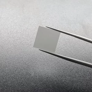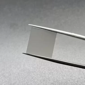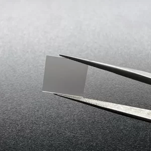
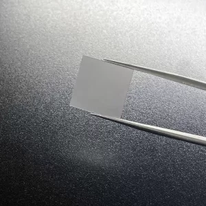
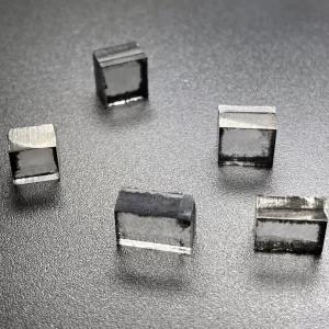
4mm*4mm Single Crystal CVD Diamond Plate 0.5mm Thickness
4mm*4mm Square Shape Optical Grade Single Crystal CVD Plate For Making Tools
Single Crystal CVD Plate Description
Chemical vapor deposition (CVD) is a common method for the preparation of thin film materials. It uses the chemical reaction of vapor precursor under specific conditions to deposit the required thin film materials on a specific substrate. In the preparation of large single crystal diamond materials, methane and hydrogen are usually used as precursors to grow single crystal diamond by vapor phase epitaxy at high temperature (about 1000 ℃), atmospheric pressure (1 ATM) or low pressure.
All along, the preparation of diamond is an important material science research topic. It’s not just that diamonds are expensive jewelry. The more important reason lies in the importance of diamond in many fields, such as: diamond itself has high hardness and high thermal conductivity, which has important industrial application value in cutting, high pressure and other fields; The study on the growth of diamond is helpful to the understanding of geochemistry; Diamond color centers have potential applications in quantum information.
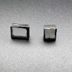
Surface: As Grown Or Laser Cut
Thickness: 0.5mm
Edge: Laser Cut or Polished
Size: 4*4mm, can customize
Application: For Making Tools
Crystal Orientation: 100 110 111
Single Crystal CVD Diamond Plate 0.5mm Thick

The process of creating Single Crystal CVD Diamond Plates is a highly efficient method for manufacturing high quality diamond products. During the process, structures and diamonds are formed in a controlled environment. Diamond structures are created by a process called lithography. Once the diamond structure is formed, the process of CVD is repeated several times to create the desired shape. This type of diamond plate is ideal for many different applications.
Characteristics of CVD diamond
A CVD diamond is a material that has been engineered for tools and high-wear components. Its fracture strength is measured with a three-point loading technique. The fracture strength of polycrystalline CVD diamond plate is as high as 2200 MPa, depending on its thickness. As the plate thickness increases, the fracture strength declines, with the substrate side suffering a factor of two less stress than the growth side.
To achieve a high degree of surface roughness, the CVD process involves the deposition of two layers of hard mask material. The first exposure of the diamond substrate uses an Al adhesion layer that has an optimal hard mask adhesion. A second development exposes the central region of the CVD diamond plate. This two-cycle photolithography process enables the creation of complex shapes that have high-resolution features.
In order to understand the growth of a CVD diamond layer, it is important to consider the formation of the atom lattice structure. The lattice structure of a diamond molecule consists of double unit cells of carbon atoms. In the CVD process, the first face (the 100) is made up of red atoms, while the second face (the 110) is formed by blue atoms.
The pressure-induced unfolding of the CVD diamond layer is controlled by adjusting the pressure. The R g of a CVD diamond plate 0.5mm thick shows 400 direction symmetric reflections. The final R g of this CVD diamond is 30 A. This value is a significant improvement in the mechanical properties of the CVD diamond. These results show that CVD diamonds are an excellent material for SAXS windows.
A CVD diamond plate 0.5mm thick can be used in many optical applications. Several advantages of a CVD diamond plate over a conventional one are described below. The CVD method produces diamonds with a non-planar structure that has an apex and an outer periphery. The two bodies are made from the same material and are bonded together with a cooling channel.
Etch depth limitation in diamond
High-precision photolithography can be used to improve etch depths of single crystal diamonds. Using a high-grade steel structure as a hard mask, etching a single crystal diamond plate 0.5mm thick reduced the top surface patterns by 5.7 um on each edge. This process also improves surface roughness to better match the requirements of optical components.
Compared to CVD processes, high-temperature gas phase etching techniques have been used for etching diamond. Hydrogen-argon plasmas have been shown to be highly effective in etching diamond substrates. Hydrogen-argon plasmas, which have low reactivity, are particularly useful for etching diamond substrates. In particular, WO 01/96633 discloses the use of hydrogen-argon plasmas at high temperatures.
Single crystal CVD diamond is considered substantially free of residual damage if the etch depth is less than 50 nm. Similarly, in polycrystalline CVD diamond, the etched depth limit is less than 20 nm. Typically, this value is about 100 mm. Further, the surface roughness Rq of single crystal CVD diamond is usually less than 0.5 nm.
The etching morphology of HPHT and CVD seed substrates differed in the extent of different growth sectors. In CVD, the dislocation density was less than half of the HPHT seed substrate. These differences made it possible to grow diamond with a higher etching quality. If you’re looking to improve the quality of your CVD diamond substrates, this technique is for you.
Surface preparation is an important process in CVD and epitaxial growth. Etching removes a layer of material from the surface. The thickness of this layer should be at least 0.2 mm or higher. The resulting surface damage layer should be the same thickness as the final thickness of the diamond grit particles used for the final stage of lapidary processing. For example, a 0.5 mm thick single crystal CVD diamond plate is only able to undergo the etching process up to 0.5 mm thick.
The method of the invention provides a diamond surface etched with at least a two-nm layer of material. The diamond surface is preferably a single crystal CVD diamond. The method of the invention is compatible with conventional lithographic processes, and it can be applied to natural single crystal diamond, HPHT diamond, CVD diamond, and polycrystalline diamond. While the method of the invention is ideally suited for producing diamond surfaces of these thicknesses, it is capable of producing a high-quality plate.
Optical properties of CVD diamond
Optical properties of CVD diamond plate have been measured using the three-point loading method. CVD diamond plate h = 0.05-1.0 mm has an average crystallite size varying by about a factor of two between growth and substrate sides. Fracture strength of the thinnest plate approached 2200 MPa. With increasing plate thickness, fracture strength decreases to a factor of two less.
The process for forming this material involves the deposition of an Al adhesion layer between the diamond and the handling wafer. In two-step photolithography, this thin Al layer prevents the diamond from cracking and is also a useful edge-bead removal method. When etching is completed, the fabricated components are released from the diamond with ease. The sidewall roughness was found to be approximately 200 nm.
The first step was to prepare the CVD diamond plate. It is a thin plate that exhibits good optical properties. The diamond layer can be used to produce laser-cut devices and optical components. The final 0.5mm thick CVD diamond plate is an ideal substrate for various applications. The material’s optical properties are well-understood. It is transparent in the UV-Vis range.
Optical properties of CVD diamond plate are improved. The topography is more uniform in the undoped CVD diamond, while the nitrogen-rich single-crystal CVD diamonds show more variations in scattering at different locations. The plate is also X-ray-topped. Optical properties of CVD diamond plate 0.5mm thickness are similar to those of natural diamonds.
The adapted growth conditions of the CVD diamond plate improve the doping efficiency of the material while preserving the crystalline quality. A higher NV/Ns ratio is a major advantage. The NV/Ns ratio may play a crucial role in the adoption of diamond and could also improve industrial production processes. The improved CVD diamond plate 0.5mm thickness could have a profound impact on the way we see and use diamond in our everyday lives.
The NV centre limits the ESR linewidth. Other colours and centres may cause problems. However, the NV centre is the focus in this case. It has a wavelength of 637 nm and a refractive index of 2.4. The NV centre is an optically active defect. A low density of nitrogen impurities makes the diamond plate optically active.
Raman/photoluminescence spectrum of CVD diamond
The Raman/photoluminescence spectrum of a CVD diamond plate 0.5mm thick was measured by using a confocal microscope. The photoluminescence signal was collected by the microscope objective and routed through a fibre to a monochromator. The intensity of the spectra was measured using a photomultiplier tube. The Raman/photoluminescence spectra were acquired under identical excitation and detection conditions and normalised to the amplitude of the first order Raman line.
The NV/PL spectrum demonstrates that a CVD diamond plate 0.5mm thick has high density of vacancies in its structure. The NV/PL spectra of CVD diamond is dominated by the NV-emission peak at 1332 cm-1. The NV peak can be easily located using a Raman spectrometer. The absence of the NV/PL peak at the Al-contact edge indicates the presence of vacancies in the film.
The NV/PL spectrum of a CVD diamond plate 0.5mm thick has strong free exciton emission at 77 K and is quenched by point and structural defects. The strong FE emission intensity is indicative of an absence of substantial defects and impurities. The NV/PL peak at room temperature corresponds to a high formation efficiency of 10%.
The voltage applied to the diamond must be below the mobility threshold to obtain the maximum charge. This voltage is approximately two orders of magnitude below the breakdown voltage of 35 cm/mm of diamond. This measurement has the potential to identify the optimum voltage range for CVD diamond production. The applied field is also critical, as it is essential to maintain the applied field below the threshold value. Alternatively, a high voltage may not be sufficient to produce a good sample.
For further analysis of the CVD diamond plate, the injected CVD sample is patterned by sputtering semi-transparent Ti contacts onto both sides. Semi-transparent Ti contacts are then patterned on the diamond plate using standard photolithography techniques. The resultant CVD diamond plate has a resistance of approximately 2.2 MPa/mm. m.sup.1/2.
4mm*4mm Single Crystal CVD Diamond Plate 0.5mm Thickness