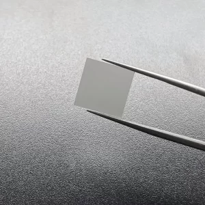
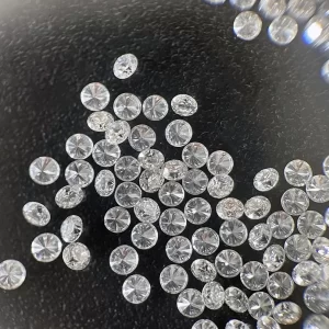
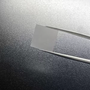
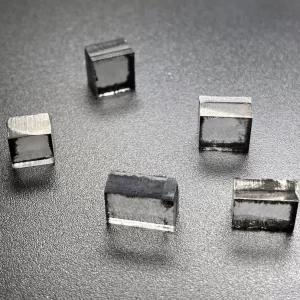
3mm*3mm Single Crystal CVD Diamond Square Shape Optical Grade
3mm*3mm Square Shape Optical Grade Single crystal CVD diamond
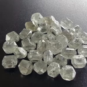
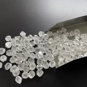
Single Crystal CVD Plate Description
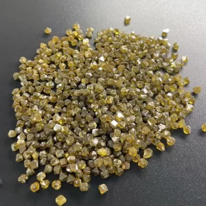
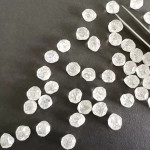
Chemical vapor deposition (CVD) refers to the gas-phase reaction at high temperature, such as the thermal decomposition of metal halides, organic metals, hydrocarbons, hydrogen reduction or chemical reaction of its mixed gas at high temperature to precipitate metal, oxide, carbide and other inorganic materials. This technology is characterized by: high melting point material can be synthesized at low temperature; The morphology of precipitated materials is single crystal, polycrystalline, whisker, powder, film and so on. It can be coated not only on the substrate, but also on the surface of powder. Especially, high melting point materials such as single crystal diamond can be synthesized at low temperature.
Microwave plasma chemical vapor deposition (MPCVD) is an important method for the preparation of single crystal diamond. In the process of single crystal diamond growth by MPCVD, the single crystal diamond substrate is directly placed in the microwave plasma chemical vapor deposition equipment for growth. Due to the high edge temperature of single crystal diamond substrate, polycrystals will be generated at the edge during the growth process, With the development of diamond growth, polycrystals at the edge will gradually invade the surface of single crystal diamond, and then reduce the effective area of single crystal diamond. After the completion of diamond growth, polycrystals around the diamond need to be removed, resulting in a lot of waste of single crystal diamond. Therefore, it is very important to avoid the appearance of polycrystalline diamond in the growth process for the growth of gem grade large-size single crystal diamond.
Crystal Orientation: 100 110 111
Type: Optical Grade
Thickness: 0.5mm
Size: 3mm*3mm
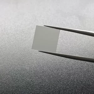
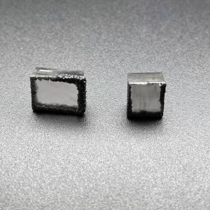
3mm*3mm Single Crystal CVD Diamond Square Shape Optical Grade
Single Crystal CVD Diamond
What is Single Crystal CVD Diamond? This article will discuss the definition, GIA, growth process, and characteristics of single crystal diamond. In addition, it will discuss the process of enlargement and compression of large samples at ultrahigh pressures. To learn more, check out the links below. Also, check out our other articles on diamonds! We hope you find this article useful! Happy shopping! And, if you are looking for a beautiful diamond for yourself, consider purchasing one of our single crystal CVD diamonds!
Optical centres
Optical centres in single crystal CVD-diamond are the result of the incorporation of optically active colour centers into the membranes. This robust and scalable approach has led to new avenues in the development of advanced nanoelectronic and optomechanical devices. This study highlights the significance of plasma assisted Chemical Vapour Deposition as a key enabling technology. The study further demonstrates the feasibility of developing single crystal diamond LEDs.
Optical centres are a key characteristic of diamonds. While NVs have narrow colour centres, their coherent properties are inferior to those of NVs. However, the NV/Ns ratio can be improved through annealing and irradiation procedures. These improvements would contribute to a more reproducible industrial production. However, the process of creating these diamonds is still technically challenging.
Optical centres are a key feature of diamond, and they define its optical properties. Moreover, irradiation can also create or modify these centers. In the present study, we have investigated the radiation hardness of luminescence centers in homoepitaxial single crystal CVD diamond, while following the evolution of photoluminescence and ionoluminescence after 2 MeV proton irradiation.
NV centers are associated with a broad range of absorption bands. At low temperatures, the NV center absorption band is correlated with emission associated with the NV centers at 575 nm. However, the NV absorption band at this wavelength is wide, and does not coincide with electron-phonon bands at 638 nm. Therefore, NV centres are difficult to directly correlate with this feature.
The presence of Pb-related color centers in single crystal CVD diamond has been demonstrated through ion implantation. Pb-based implantations of single crystal CVD diamonds have produced promising results, and the presence of these centres has been shown to be a significant indicator of a stable Pb-based defect in the diamond. It has also been shown that Pb-related color centers are correlated with the implantation fluence.
Growth process
One of the most remarkable materials for medical therapy and radiation harness is single crystal CVD diamond. Researchers have developed a novel growth process for CVD diamonds. In the process, diamond is grown on a plasma substrate under various parameters, such as pressure, temperature, and methane concentration. A plasma substrate is laser cut into 0.5 mm-thick pieces, and the samples are then grown in a reaction chamber using 3% methane.
The XRD analysis confirms the single crystal nature of the grown CVD diamond. It shows that the diamond substrate is oriented in the direction of growth, with the lateral growth occurring on a hundred-facet substrate. Moreover, this lateral growth process reduces dislocation density. Tallaire et al. have shown that growth of single crystals can be facilitated by a hole in the substrate.
A recent study used microwave plasma CVD to grow diamond films on the different facets of a synthetic IIa-type SC HPHT diamond. In this study, the diamond films were grown on the facets of a beveled SC diamond, which has low index 100, 110, and 111. Other planes showed the growth of nanocrystalline diamond films. Therefore, a single-crystal diamond (SC) can be used as an optical element in quantum devices such as computer chips.
The results obtained showed that the plasma-covered region showed high concentrations of carbon and high methane concentrations. The resulting films had a high degree of morphology and were characterized by a wide range of growth step spacings. The diamond samples have sharp peaks near 1332 cm-1 in the Raman spectra, which were correlated with etch pits on the surfaces. However, this study does not explain the growth process of single crystal CVD diamond films.
Characteristics
A variety of processes are used to grow single crystal diamonds. Generally, these processes use CVD growth parameters that favor the growth of single crystal diamonds. For example, in polycrystalline CVD diamond processes, the CVD process uses plasma that is uniformly distributed over the growth surface area. Nevertheless, in single crystal CVD diamond growth processes, the plasma can be a little diluted. This can make the growth process more efficient.
The growth of nitrogen-doped multilayers on an HPHT seed substrate has also been achieved. These thin CVD diamonds are more fracture-resistant compared to single-crystal diamonds made on an HPHT seed substrate. These new developments may allow the production of nitrogen-doped single-crystal diamonds in even higher power densities. These diamonds may have improved fracture toughness compared to unintentionally doped CVD diamonds.
Non-uniformity in growth rate, cracking, and impurity content may also occur in single-crystal CVD diamonds. These variations may occur as a result of the chemistry of CVD diamond growth. Temperature variations, for instance, can affect the rate of impurity uptake and crystal morphology. Furthermore, these differences can be lateral or parallel to the growth direction.
In addition to nitrogen-doped single-crystal CVD diamonds, the study also showed that the incorporation of nitrogen impurities was influenced by substrate orientation. Moreover, the misorientation angle affected the nitrogen incorporation. For this reason, several nitrogen-doped layers were designed to grow on one sample, and the growth conditions were altered from layer to layer. This proved to be a reliable tool for the study of nitrogen-doped CVD diamonds.
GIA
In the early stages of diamond-making, CVD samples were brownish. Then, producers discovered that they could remove this coloration by treating the diamonds under high temperatures and pressures. However, it is important to note that CVDs also have signature features that make them distinguishable. The GIA has established criteria for identifying diamonds with these features, including the color of the diamond’s crystals.
Since then, researchers at the GIA have observed parallel bands in GIA CVD samples. These bands indicate interruptions in the growth sequence. When CVD grows too long, the crystal becomes polycrystalline. Hence, it is important to remove the crystal from the reactor, polish away the polycrystalline diamond, and then continue the growth process. In addition, the chemical composition of a diamond at start-up and steady-state differs slightly. This means that the GIA diamond graders cannot use the same terminology for the two types of facets.
The GIA Laboratory observes a gradual increase in clarity grade for CVD samples over time. These diamonds exhibit the characteristics of natural diamonds with higher clarity grades. The inclusions typically consist of clouds, pinpoints, and black “crystals.” They are not diagnostic enough to be used for identifying a CVD diamond. However, Type II diamonds should be sent to a lab for analysis. The GIA Laboratory also notes that major CVD manufacturers usually inscribe the origin of their synthetic diamond on the girdle. If the stone does not have such an inscription, it may be a natural diamond.
The processing of diamond crystals took place under high pressures and temperatures. Nitrogen added during the gas phase increased the growth rate of the doped layer and the buffer layer. The resultant material was a diamond with large pyramidal and conical shapes. Photoluminescence imaging and Raman mapping revealed a zero phonon line (ZPL) at 575 nm. After this, the crystals were cut and polished for GIA certification.
IGI
IGI single crystal cultivated diamonds are a new type of gemstone with outstanding clarity and color grades. The synthetic diamonds are grown in a lab and undergo a series of tests. Once they are grown, the diamonds undergo high-temperature treatment, which enhances their color and transparency. IGI has detected parcels of these diamonds and will test each stone to determine if it is a natural diamond.
The method used to grow single crystal CVD diamonds is characterized by active management of the morphology and a high degree of control. Temperatures in the etch phase should be reduced slowly, over hours or even days. The etch phase can be too short or too long. Using a CH4 ramp after the etch phase helps reduce the likelihood of cracking of single crystal CVD diamonds.
One of the main challenges of growing single crystal diamonds is that the growth process has many inherent risks. Defects in the substrate cause numerous dislocations, which propagate throughout the layers of the diamond. To minimize the risk of such problems, appropriate process parameters must be applied. IGI single crystal diamonds should be monitored carefully, as a high degree of control can prevent undesirable growth. They can be viewed as a valuable resource for the industry.
The nitrogen addition used in CVD single crystal diamond growth affects the morphology of the diamond. It affects its growth rate, as a nitrogen-doped diamond layer requires a lower growth temperature and a lower concentration of nitrogen. IGI single crystal CVD diamond with nitrogen doped layer is 650 nm thick and characterized by smooth surface morphology. It is also tougher than a CVD single crystal diamond.
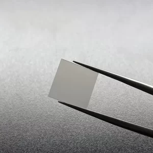
Single Crystal CVD Diamond Square Shape Optical Grade
Optical grade is defined as a quality attribute that defines the optical quality of a single crystal diamond. Its optical grade depends on the dislocation density, nitrogen content and other variables that affect the quality of the diamond. The range of this parameter varies in different production processes. However, it is consistent within the range of 1.4 to 2.6. There are also different parameters indicating the difference in optical grade due to the film thickness of the diamond.
Variations in CVD reactor conditions
The optical properties of a diamond crystal depend largely on the chemical and physical properties of its grain boundaries. In addition to the grain boundaries, diamond also contains point and extended defects. Extended defects can occur as twins, vacancy clusters, and dislocations. These defects may be either electron donors or acceptors. CVD diamond contains non-carbon atoms such as Si, P, and S.
Among other additives used, Ge can suppress the reaction that forms diamond, allowing it to grow preferentially on the seeds and produce large crystals. Ge can also be used as a catalyst in CVD reactors to enhance the growth of diamond. The chemical composition of diamond is largely determined by its optical grade, which is the most important criterion of quality. The following table summarizes the chemical composition of diamond.
The chemical composition of diamond varies depending on its size, shape, and metallisation. A typical CVD diamond has a peak power density of 100 W/mm-2, and a total thickness of 1000 nm. This material has excellent electrical and thermal conductivity. It is also a good candidate for photovoltaics, which use light from laser diodes to create a high-resolution image.
The CCE of polycrystalline diamond is approximately 50%, which is considered the highest possible value for radiation detectors. Moreover, high-purity single crystal CVD diamond has been extensively investigated for detector applications. Its high CCE can reach 100%. This material also has a good electrostatic and atomic resolution, which is important for high-resolution particle energy spectroscopy. These qualities make diamond a great candidate for photonic devices.
Variations in dislocation density
In the present study, we investigated the variations in dislocation density of single crystal CVD (SVC) diamonds of different optical grades. We used a Keithley 4200 semiconductor characterization system and a 6-circle X-ray diffraction spectrometer to study the dislocation density of diamonds. Furthermore, we used a confocal micro-Raman spectrometer to investigate the defect structures in diamond. We also used a Gemini SEM 500 to measure the dislocation density. Finally, we employed a SIMS system to investigate the concentration of nitrogen and tungsten impurities in the single crystal diamond square shape optical grade.
The length of the longest linear internal dimension in CVD diamond materials is used to determine the dislocation density. In single crystal diamonds, dislocations are located on lines that cross the growth plane. For example, in a cube, the body diagonal possesses a dislocation density of 1011, which means that a particular optical grade of single crystal diamond will have a high dislocation density.
The dislocation density of single crystal CVD diamond materials may vary significantly. For example, one crystal could have 104 dislocations per centimetre, while another may have threex103. But if the dislocation density of a single crystal diamond is low, it means that its birefringence is reduced, and depolarisation losses are reduced. Moreover, single crystal diamond materials may contain dislocations that are less than 2%, 1%, or 5%.
For example, a high dislocation density of a diamond plate may lead to increased photon flux. However, this effect can be mitigated by the use of proper crystal selection methodology. Single crystal CVD diamonds can be used as X-ray monochromator elements at synchrotrons. The dislocation density of a single crystal CVD diamond square shape optical grade may be up to 50 m compared to a single crystal CVD diamond of the same size.
Variations in nitrogen content
A study has recently shown that variations in the nitrogen content of single crystal CVD diamonds adversely affect their exceptional optical, electronic and spintronic properties. This study also revealed that the diamonds’ brown colour is caused by a defect known as the nitrogen-vacancy-hydrogen defect. To identify the defect responsible for the brown colour, electron paramagnetic resonance was used. Moreover, the nitrogen content of single-crystal CVD diamonds was estimated using a combination of optical and Raman spectroscopy.
The nitrogen-doped layer of the diamond has a higher compressive stress than the buffer layer. This defect produces a biaxial stress state and induces a peak shift in the diamond’s Raman spectra. Furthermore, it also produces a higher-wavenumber Raman spectra. Finally, it increases the stress level of the diamond by causing the diamond’s first-order phonon peak to be at a higher wavenumber.
Variations in nitrogen content of single crystal CVHD diamonds can be attributed to two mechanisms: doping and surface defects. However, the effects of nitrogen on the CVD diamond growth are still under investigation. As the nitrogen content increases with the concentration of carbon nanoclusters, the amount of absorption varies. This effect is particularly evident in the optical grade of single crystal diamonds that have a square shape.
The technique also helps understand the origin of defects in diamonds. A recent study found that variations in nitrogen content of single crystals produced by HP/HT techniques can be traced to different origins. These results demonstrate the applicability of the technique to other materials, such as single crystal CVD diamonds. The technique can also be used for studying the mechanical properties of superhard materials.
Differences in detector performance due to film thickness
Different detectors are characterized by different spectroscopic properties. These differences are due to differences in the film thickness of single crystal diamond detectors. The film thickness of single crystal diamond detectors may also influence their polarization characteristics. This paper examines differences between single crystal CVD diamond detectors and the other types of single crystal diamonds. The study also explains why different detectors have different polarization characteristics.
Single crystal diamond is the ultimate material for high voltage, temperature, and frequency applications. It exhibits excellent radiation resistance and is able to host a wide range of colorcenters, involving impurities. It is therefore a promising material for high-end detectors. But the question remains: why does this material perform better in certain applications than others? Let’s take a look at how it works.
Single crystal diamond can be microfabricated using lithography or reactive ion etching. These methods have helped improve the surface quality of single crystal diamond. The resulting components exhibit 82-93deg sidewall angles and surface roughness of 200 nm. These diamonds are also compatible with the standard thin-film deposition techniques. However, the limited size of single crystal diamond substrates prevents its widespread use in micro-mechanical components.
Differentiation in detector performance due to film thickness of single-crystal diamondsquare-shape optical grade
Applications of sc-CVD diamond
A recent study reports the first experimental results of single crystal CVD diamond plates, which are square in shape and possess a nominal optical grade of 001. The studied diamond plates have a surface area of 7 mm x 7 mm and a thickness of 1 mm. The nominal crystallographic orientation of the surface was 001, and twenty-one of the plates had an edge orientation of (100) or (110). These diamonds were characterized by using a multiwire X-ray back-reflection instrument (MCX-R) at the Cornell Center for Materials Research. The deviations of the nominal surface orientation from the actual oriented diamond were less than four microns.
The process for creating these diamonds began with a membrane window, which allowed the researchers to observe the diamond quality during fabrication. Using a 532 nm laser, they measured the Raman spectra of the single crystal diamond and sp3 bonded carbon. These materials have a full width half maximum of 13.33 cm-1, which is comparable to the 2.3 cm-1 of bulk SCD. After ion implantation, the diamond no longer has the peaks at 1333 cm-1, but new peaks appeared in the spectrum of the ion-implanted crystal.
The reduction of defects is important for several applications. The presence of defects, such as dislocations and point defects, reduces the CVD diamond material’s thermal conductivity. In addition, point defects interfere with the absorption of light and reduce optical transparency. Dislocations, on the other hand, cause local birefringence, which disrupts the cubic symmetry of the lattice.