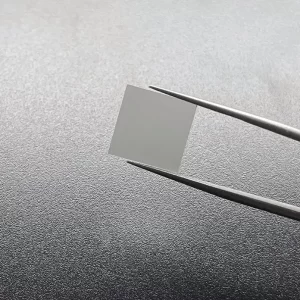
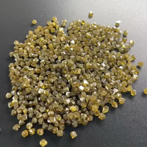
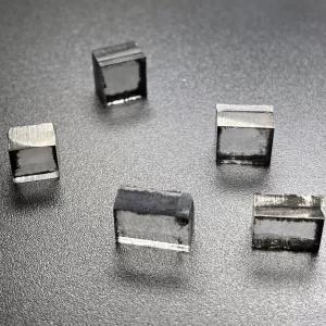
5mm*5mm Square Shape Optical Grade CVD Single Crystal Plates For Making Tools
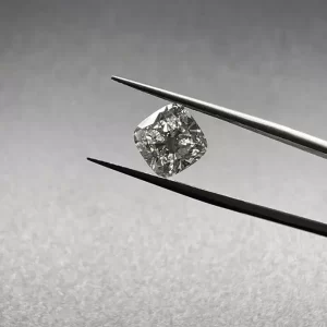
CVD Single Crystal Plates Description
Diamond has high hardness, chemical inertness, optical transparency, high thermal conductivity and electrical insulation. Because many applications recognize the benefits of this material. In particular, it is required to meet the requirements of industries involving extremely high power density, high mechanical load or severe wear conditions.
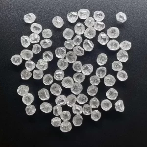
The growth conditions of diamonds cultivated in the laboratory are similar to those of natural diamonds. Natural diamonds are deeply hidden in the earth and grow with geological changes under high pressure and high temperature. Finally, the diamonds move to the surface of the earth through molten rock. A similar situation was created in the laboratory, the same chemical evaporation and pure carbon, chemical and optical properties of natural diamonds. Even if these diamonds are man-made, everything in these diamonds, from the internal atomic structure to the sparkle, is exactly the same as natural or mined diamonds.
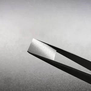
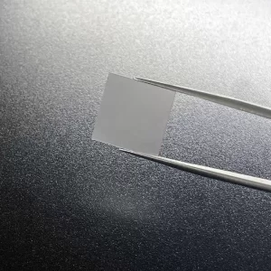
Surface: As Grown Or Laser Cut
Thickness: 0.5mm
Edge: Laser Cut or Polished
Size: 5*5mm, can customize
Application: For Making Tools
Crystal Orientation: 100 110 111
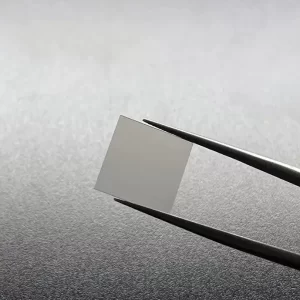
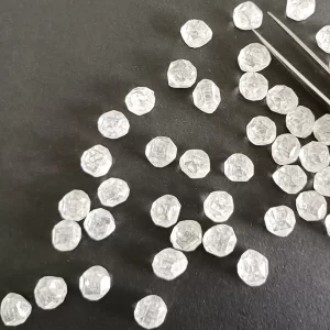
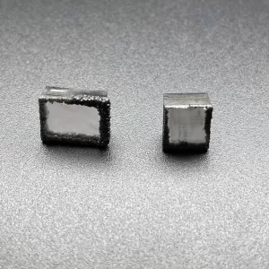
White CVD Single Crystal Plates
We have successfully fabricated White CVD Single Crystal Plates. Using a rotating anode X-ray source, we have achieved high dislocaiton density. The high dislocaiton density has been confirmed by X-ray diffraction imaging. This work has implications for the fabrication of other semiconductor materials, including refracting monochromators. We thank J.D. Brock for his support and discussions and D. Sagan for his assistance.
Process parameters for obtaining a smooth, single crystal CVD diamond surface
A single crystal diamond can be produced by adjusting several process parameters. For example, temperature can vary from 700 to 1500 degrees C, depending on the type of single crystal. At higher temperatures, polycrystalline diamond can be formed. At lower temperatures, diamond-like carbon may form. Temperature gradients should be less than 20 degrees Celsius, or less than 1 degree Celsius. A smooth surface is the result of the correct process parameters.
The hard mask layer is deposited in two steps to eliminate edge beads and ensure a smooth diamond surface. The first exposure, using a 0.5-mm-wide frame, uses a high dose adapted to the bead’s thickness. The second exposure removes the edge bead and completes the process. The final product exhibited a smooth, single-crystal CVD diamond surface with sidewall angles ranging from 82 to 93 degrees.
The next step involves polishing. Using a pure oxygen plasma, the micromasking effect was reduced. This technique exhibits high etch rates and excellent diamond selectivity. One challenge with this technique is the high amount of hard mask and poor adhesion of silicon oxide layers to the diamond surface. Nevertheless, it has a number of advantages, including smooth and uniform surface.
Reactive ion etching improves surface roughness. Reactive ion etching improves surface roughness by up to 20 nm. The improved surface quality can be used for optical components. This paper reviews the latest research in this field. The results obtained show that the etching process can be used to produce single crystal diamonds with an improved surface roughness.
The experiment showed that this method is possible to mass-produce single-crystal needle-like diamonds. This is crucial for practical applications of single-crystal diamonds. However, this process is still in its early stages. This paper will examine this process in further detail. The final goal is to determine which process parameters can lead to the best results. When these parameters are optimised, the resultant diamonds will have the best possible surface finish.
X-ray diffraction imaging
The X-ray diffraction imaging technique was applied to investigate the lattice distortion of white CVD single crystal plates. A narrow collimation slit was used to limit the incident beam to a ten-um strip. The X-ray beam and the crystal then intersect at the intersection point, resulting in a virtual two-dimensional slice. The resulting image shows the local lattice quality in the topographic image.
The two dominant effects attributed to the distortion of the reflected radiation are the intrinsic effective curvature of the crystal lattice along the footprint of the incident beam and the increase in radiation divergence caused by local interactions with misoriented crystal blocks. These two effects are coupled by stress-strain elasticity relationships. As a result of CVD growth, the lattice is bent, resulting in a local change in lattice parameters. Locally, the largest contribution to the reflected radiation wavefront is due to the large curvature of the lattice, which cannot be controlled during CVD growth.
The results showed that the topography of Type IIa white CVD single crystal plates is influenced by the overgrown boron-doped layer. The X-ray topography showed that the bulk substrate was dislocation-free before the boron-doped layer was overgrown. Additionally, the boron-doping layer caused non-homogeneity across the surface. The presence of these chaotic features indicates that the crystal growth process had not been homogeneous across the entire surface.
X-ray diffraction imaging has several disadvantages. The technique can only examine a fraction of the specimen at a time. Its primary limitation is that it cannot determine the quality of the entire specimen. In addition, the technique cannot distinguish the orientation of the single crystal because of incoherent, fluorescent, and temperature-diffuse scattering. In addition, the technique is limited to thin specimens.
In addition to analyzing sample shape, X-ray diffraction images can also reveal defects within the white CVD material. For example, the FWHM map for Sample 8 reveals that the sample topograph is dramatically distorted. This shape distortion is caused by the curvature of the sample. Besides the sample surface, the thickness and concentration of the overgrown boron-doped layers are factors that determine the global curvature. The overall curvature of the white CVD single crystal plate translates to deformation of the entire diffraction image.
Characterization of point defects
Characterization of point defects in white CVD composites involves measuring the dislocaiton density. To do this, a Cu K rotating anode source is used. The plate was oriented with its edges parallel to the direction of the beam, as depicted in Figure 1. The data collected required a longer time, but a photon counting area detector was used to reduce the time required for data collection. The topographs used to study the crystal surfaces were noisy and therefore did not reveal point defects.
The data obtained by this method allow the measurement of the average width and standard deviation of the rocking curve. The results suggest that the refocusing monochromator is composed of a CVD diamond. The standard deviation of the peak position is about 20 rad, and the width of the rocking curve is 150 rad. The rocking curve width varies by 24 rad in each layer, with local lattice rotation contributing more than the other sources of variation.
For the CVD-N sample, additional data collection was carried out to visualize and quantify the effects of the crystal lattice distortion. Rocking curve peak position topographies reveal regions with larger variations in effective misorientation. The region of interest was selected for further analysis. In addition, the angular characteristics of this region were more uniform than those of the crystal’s entire surface. The rescaled colorbar reveals variations of about 100 rad.
The experimental setup for the study used two CVD processes. The diamond plate CVD-N has an edge orientation of (110), while the diamond plate CVD-B has an edge orientation that is oriented (110). The results of this experiment indicate that the overall distorted lattice of the CVD-N is 50 m greater than that of the CVD-B single crystal plate.
To mitigate this effect, the rocking curve imaging of CVD diamond crystal plates was performed in a double-crystal quasi-nondispersive configuration. The Si 111 DCM used in the beamline serves as beam conditioner and is monochromatic. The angles between the lattice planes are important to characterize the defects. Asymmetry is a common feature in diamond crystals.
Application of SC-CVD diamond crystals as a refocusing monochromator
The application of SC-CVD diamond crystal plates as side bounce monochromators can provide a ten-fold increase in reflected x-ray flux, according to a recent study. The CVD diamond plates were tested at the Cornell High Energy Synchrotron Source under high-heat conditions. In the experiments, the reflected beam was focused using Pt-coated mono capillary optics.
In this system, a sheath 134 is installed around a diamond 136. The sheath is made of a high thermal conductivity material. The sheath 134 tightens on the diamond 136 by a screw that is positioned in a set ring 130. Moreover, the sheath serves as a heat sink for the diamond 136. The sheath also makes thermal contact with the stage.
This diamond is placed within a region of plasma 141 at a height H above the deposition chamber floor 122. The temperature gradient between the top and bottom edges of the diamond 136 is measured and is called the resonant power. The temperature gradient is larger between P1 and P2, and it is possible to measure the amount of resonant power in a specific region.
The growth surface temperature of the diamond can be controlled by the main process controller. The temperature gradient between the growth surface edges and the growth surface middle is input to the controller. When the diamond reaches the desired thickness, the growing process can be terminated. The diamond is then repositioned into the holder. This repositioning path is called the “NO” path.
The synthetic CVD diamond has unique properties, including high spectral transmission, physical robustness, and the highest thermal conductivity. As a refocusing monochromator, this diamond has been demonstrated to be effective at delivering the desired spectral response. Further, the crystal has a large bandwidth and high sensitivity. It is expected to provide high-quality output for many years to come.
The SC-CVD diamond crystal plates used in the ATLAS detector are an excellent solution for refocusing x-rays. This material exhibits excellent radiation hardness, low charge leakage, and low-luminosity. Its low leakage current makes it a good candidate for next-generation pixel detectors. The RD42 collaboration collaborated with other groups to optimise the diamond sensor for bump-bonding. The results were impressive: a diamond-based pixel detector that was over 98% bump-bonded is operational.
5mm*5mm White CVD Single Crystal Plates For Making Tools