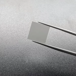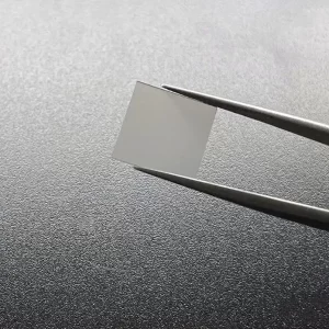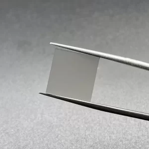
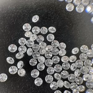
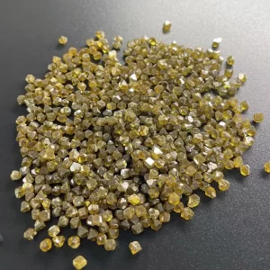
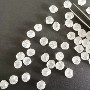
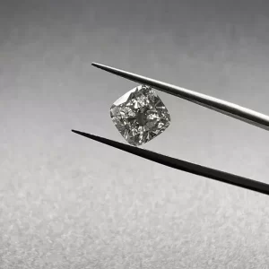
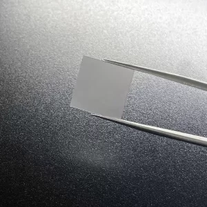
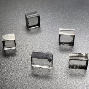
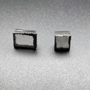
CVD Single Crystal Diamonds 0.5mm 3.0mm Thickness
Optical Grade Square Shape CVD Single Crystal Diamonds For Making Industrial Tools
CVD Single Crystal Diamonds Description
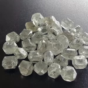
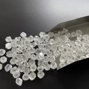
Diamond is widely used because of its excellent properties, such as the highest hardness, excellent wear resistance, low friction coefficient, high thermal conductivity, low thermal expansion coefficient and extremely stable chemical properties. CVD diamond single crystal is planar, with clear crystal edge and vertex angle.
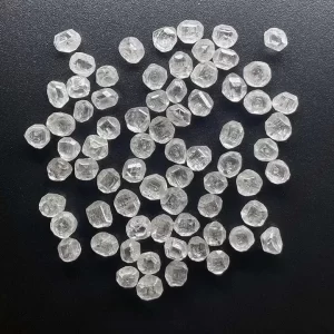
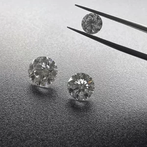
Currently we can provide different grades of CVD single crystal diamonds. Mechanical or thermal grade CVD single crystal diamonds is for industrial precise tools making. Optical grade CVD plates is usually used for optical windows, high precise tools, anvil and sensor etc. Electronic grade CVD single crystal diamonds is for quantum optics, radiation detector etc. We also can supply gem quality CVD single crystal diamonds which are used for cutting lab grown polish diamonds.
Surface: As Grown Or Laser Cut
Thickness: 0.5-3.0mm
Edge: Laser Cut or Polished
Size: 1-12mm, can customize
Application: For Making Tools
Crystal Orientation: 100 110 111
CVD Single Crystal Diamonds With Nitrogen Doping
CVD Single Crystal Diamonds are a new class of synthetic diamonds. They exhibit distinctive characteristics that distinguish them from other diamonds. For example, CVD diamonds have a full width at half maximum and a polycrystalline edge. In addition, corner magnifications show significant spherical diamond-like carbon in the corner. In addition, the top edge of the diamond is sharp. Further, polishing of the black diamond-like carbon widens the XRD peak width.
Molybdenum
The crystals were grown by a microwave process using a 6-kW power and 2.45 GHz frequency. After initial rotation, the crystals grew vertically. They had no lateral growth, which may be the main reason for the high quality of the final product. The growth process was repeated several times, with each new sample exhibiting a different crystal quality. Fig. 11 shows the changes in the internal stress and crystalline quality. The central region had the highest stress value and higher crystalline quality than the edge region, which was observed only for 0.5 mm and 1.5 mm.
During the growing process, oxygen is added to the CVD stage. This process removes impurities that are related to nitrogen. Oxygen helps reduce hydrogen and silicon content in the material. The result is a CVD layer with a lower growth rate of 10 mm/h than a standard process that yields about 0.3 mm/h. Further, molybdenum is incorporated into the crystals during the process.
After the forming process, the Mo-diamond composite is formed by fusing Mo and MoS2 layers. MoS2 layer changes the Raman spectrum of diamond substrate. Mo2C Raman lines are most intense at 800 and 1000 cm-1. This property makes these diamonds suitable for high-quality applications. These materials may also be used in solar cells, water disinfection, and water splitting.
Tungsten
A new method of growing CVD Single Crystal Diamonds in Tungstenem is described in this article. The technique involves growing a diamond layer on a synthetic substrate of 6×6 mm in several stages. The growth rate of each stage increases the area fraction of faces with minimum growth rate. This parameter is called alpha-parameter a and is equal to three and a half V100/V111. The greater the alpha-parameter a, the larger is the area fraction of 111 face.
The diamond anvils used in this method are sized at about 300 mm in diameter. The first stage of the process involves covering the anvils with a tungsten mask. The second stage is performed by compressing the tungsten film between two NCD micro-anvils. In this step, researchers can determine the sp3-diamond content in the anvils by performing Raman spectroscopy and micro-focused X-ray photoelectron spectroscopy.
NCD is grown using chemical vapor deposition on diamond anvils. The gas phase chemistry of the CVD method includes 9% CH4/H2, 10% N2/CH4, and a substrate temperature of 830 degC. The tungsten mask serves as a deterrent for growth of diamond elsewhere on the diamond anvil. The tungsten mask is then removed and the NCD micro-anvil is exposed. This high-resolution image of the CVD grown second stage was obtained using scanning electron microscope (SEM). The average grain size of the NCD micro-anvil is 115 nm.
Nitrogen in-situ doped diamond matrix
The doping efficiencies of nitrogen are highly dependent on the growth condition and the crystal orientation. Nevertheless, the tunable controllability of nitrogen makes it a promising material for several applications. Single crystal diamonds with nitrogen in-situ doping can produce NV0 defects in their vertical growth sector. Furthermore, they can be integrated into devices. Here, we will discuss the advantages and disadvantages of nitrogen doping in single crystal diamonds.
The NV0 defect is characterized by a peak shift of 1332.6-1335.5 cm-1 and a fluorescence intensity of 3200 counts. Several other defects were also identified including a cluster of nitrogen-related defects in the pyramidal region of the single crystal diamond. The unintentionally doped CVD single crystal diamonds have lower fracture toughness compared to the HPHT seed substrate. Further research will be conducted to make CVD single crystal diamonds with higher fracture toughness.
Single-substitution nitrogen readily incorporates into synthetic and natural diamonds. It preferentially locates into 111 and exhibits behavior similar to deep donors. The nitrogen atoms are charged and undergo annealing based on their energy, which is -1.7 eV below the conduction band minimum. During diamond growth, nitrogen-related defects become neutralized within a few ns.
Growth on recessed carrier substrate
A recessed carrier substrate is a suitable choice for CVD single crystal diamond growth, as it allows for temperature control and enables the use of diamonds of various origins. The process is sensitive to the height above and below the carrier substrate, and it is generally unsuccessful at initial heights below 2 mm. However, it is possible to overcome this problem by placing spacer wires between the carrier and the recessing plate.
In CVD single crystal diamond growth on recessed carriers, the seed with the largest side-to-side width grows to a height of 10 mm between the two sides. The morphology of the single crystal diamond is investigated by characterizing its vertical cross section. The two growth fronts of the carrier substrate converge at the coalescence zone, forming a crystal with a broadened face and a narrowed top-face.
The second CVD process enables the single crystal diamonds to be removed from the recessed carrier substrate. They are then mounted on a new recessed carrier substrate that has a deeper recess. A third CVD single crystal diamond growth process is used to increase the thickness of the plurality of single crystal CVD diamonds. It is this process that leads to a low-birefringence single crystal diamond.
Mechanical properties
CVD single crystal diamonds have a dislocation density less than 104 dislocations per cm2. These materials may contain up to 3×10³ dislocations per cm2 or even 10 dislocations per centimeter. This decreased dislocation density reduces the birefringence and depolarisation losses of the material. The resulting material is a high-quality diamond. The mechanical properties of CVD single crystal diamonds are characterized by the following four characteristics.
The longest linear internal dimension is the distance between the two faces of a CVD single crystal diamond material. The critical angle is the angle measured relative to the direction normal to the surface of the material. The CVD single crystal diamond material can be more than 30 mm thick and still exhibit the required mechanical properties. CVD single crystal diamonds can be thinner than 1 mm or thicker than 20 mm, 7.5 mm, or even 10 mmm.
The growth rate and morphology of CVD single crystal diamonds are influenced by the concentration and temperature of nitrogen added. Adding nitrogen will increase the growth rate of CVD single crystal diamonds with a thin layer. Sample 2 was grown by intentional addition of 0.09 sccm of N2 and grown at a lower temperature (880 degC) for a shorter period of time. Despite its relatively low growth rate, sample 2 shows a smooth surface and a 650-nm thick nitrogen-doped layer.
Impurities
In this study, we examined the effects of nitrogen addition on the morphology of CVD single crystal diamonds. The etching morphology of the HPHT and CVD seed substrates differed in the extent and number of different growth sectors. We found that nitrogen-doped CVD single crystal diamonds grew at a lower temperature and with a lower concentration of nitrogen. In our experiments, we deliberately added 0.09 sccm of N2 to a single sample. Moreover, we used the same growth condition for the growth of a CVD single crystal diamond, but we changed the growth temperature and time of each layer.
In a diamond grown using CVD, the centre is NV for clarity. Any other colour centre may pose issues. The presence of NV defects limits the ESR linewidth. These defects are the most common type of defects that limit the spectral response of a diamond. They also limit the ESR linewidth, which measures the number of detected photons. In a diamond resulting from CVD, NV centres represent a majority of the diamonds.
The nitrogen-vacancy-hydrogen (NVH) spin in CVD diamonds is the strongest signal of impurities. The spin readout contrast is reduced to less than 1% in the presence of large ensembles of NV defects. Similarly, a diamond crystal with a high nitrogen content displays a long spin coherence time and a high negative charge state. The nitrogen-vacancy-vacancy (NVH) spin is another type of defect that is highly desirable for use in particle physics.