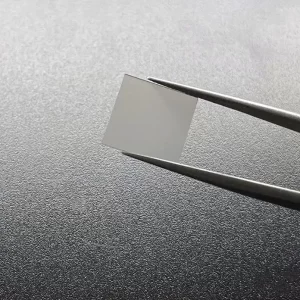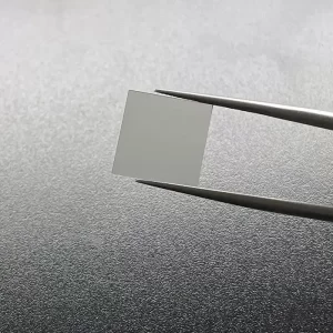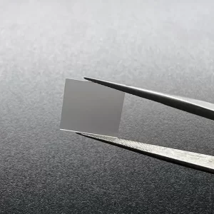
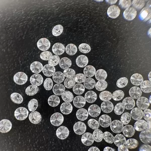
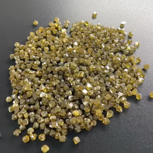
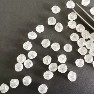
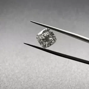
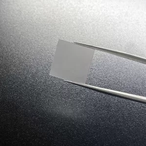
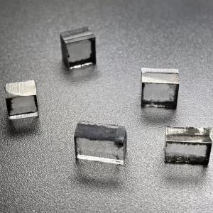
15mm*15mm CVD Single Crystal Diamonds Polished Edge
15mm*15mm Square Shape Optical Grade CVD Single Crystal Diamonds
CVD Single Crystal Diamonds Description
Due to the inherent transparency of CVD Single Crystal Diamonds in a wide wavelength range, optical characterization has long been a common method to characterize inclusions, impurities and color defects.
CVD Single Crystal Diamond has the widest optical transparent band of all known solids, ranging from 0.22um to far infrared. Only the intrinsic vibration absorption band with intensity between 2.5 and 7um interferes with the transmittance of CVD Single Crystal diamond in the infrared region. CVD Single Crystal Diamond is transparent in ultraviolet, visible and infrared spectra, which provides many opportunities for lattice defects to reveal the optical activity of electronic and vibrational transitions. Large band gap energy (5.49 EV) is a particularly favorable condition for luminescence, because the ground state and excited state are required to be in the band gap for radiative electron transition. The high mechanical hardness and thermal conductivity of CVD Single Crystal Diamond greatly support its optical applications, making CVD Single Crystal Diamond optics very stable and wear-resistant in many aspects. When discussing the optical properties of materials, we should carefully consider their optical centers, because their properties and abundance determine almost all the optical properties of materials. In addition, the optical center content is the main parameter to characterize the optical properties of materials. So far, more than 150 vibration centers and more than 500 electron optical centers have been detected in CVD Single Crystal Diamond, with the spectral range of 20-0.17um.
Surface: As Grown Or Laser Cut
Thickness: 0.5mm
Edge: Laser Cut or Polished
Size: 15*15mm, can customize
Application: For Making Tools
Crystal Orientation: 100 110 111
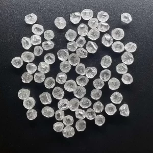
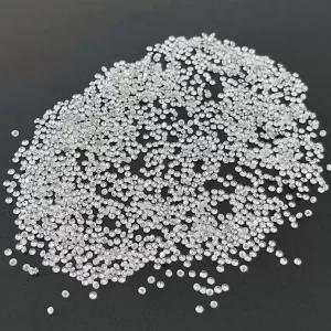
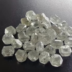
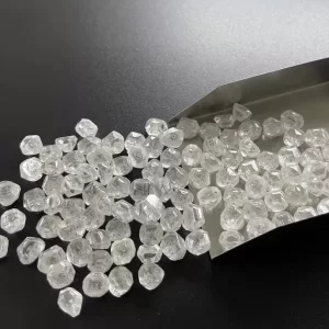
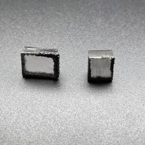
CVD Single Crystal Diamonds – Polished Edge and Rough
What Are the Differences Between Polished and Rough CVD Single Crystal Diamonds? This article discusses the differences between these two types of diamonds and explores the various factors that influence their appearance. In addition, this article covers the various aspects of polishing and the Absorption coefficient. In addition, this article provides some information on the different types of surfaces for these diamonds. Ultimately, the CVD Diamond polishing process will help you to get the most beautiful and affordable piece of jewelry.
Birefringence of CVD diamonds
A chemical vapour deposition (CVD) diamond is the result of a process that creates a layer of carbon nanoclusters on a growing surface. Researchers have examined the polarization properties of the CVD layer on a polished edge and a flat surface. High-order birefringence in a diamond is dependent on the dislocation density, and the higher the density, the higher the occurrence of abnormal birefringence.
A CVD single crystal diamond has a brownish color. The plasma ball was adjusted by vertical movements of the sample holder. In addition to measurements based on Raman scattering, optical and X-ray spectroscopy methods were also used to analyze the dislocation density. The results indicate that a CVD diamond grown by DC arc plasma jet CVD is an excellent candidate for applications in quantum computing.
The growth process of CVD single crystal diamonds often results in strain-induced birefringence. This is caused by bundles of edge dislocations that change in length and intensity with the polarizer’s rotation. For example, in parallel polarizers, four bright petals appear on the polished edge of a diamond while the other eight show a dimmer spectrum. This specific arrangement of dislocations is explained by the isotropic elasticity theory.
The results of the experiment have shown that the SF6-based recipe produces a 2.5-mm thick membrane along the outer edge of the diamond. A measurement was performed using a LeXT OLS4100 LSM with a 405 nm laser. The results of the test were published in Proc. R. Soc. L. A Dec. 8, 1996 452:2751-2765). A similar method has also been used to measure the birefringence of CVD single crystal diamonds.
Absorption coefficient
The thermal conductivity of single-crystal diamonds can be measured by measuring the temperature of the edges. The absorption coefficient of diamonds can be measured with the help of a thermal conductivity meter. Various types of diamonds have different thermal conductivity. The material used to manufacture them differs in size and shape. For example, the roughness of a diamond is a factor that affects its thermal conductivity.
CVD single-crystal diamonds have a low absorption coefficient. This feature makes them suitable for use in extreme mechanical and thermal applications. The optical properties of CVD diamonds are essential for these extreme applications. These experiments have been conducted on three CVD diamond plates, two of which are produced by Element Six BV Co and one by IAP (N.Novgorod). All three samples had different absorption coefficients.
The workshop also included sessions on electronic transport measurements of CVD single-crystal diamonds. These two workshops were organized by NIST. Participants’ feedback was used to determine the topics for the second workshop. Besides NIST researchers, government scientists and university scientists were also invited as experts in measuring these properties. As a result, 44 people attended the workshop. Moreover, the workshop provided valuable information to other participants.
The aforementioned parameters affect the growth rate of CVD single-crystal diamonds. The growth rate of a diamond is the distance moved by the growth surface per unit time. The hkl and uvw crystallographic directions are used to describe these characteristics. The diamonds deposited in a single-crystal reactor are homoepitaxial in nature. They have no internal imperfections.
Surface roughness
The surface roughness of CVD Single Crystal Diamonds is controlled by the micromechanical components’ sidewall profile. These micromechanical components are characterized by the surface roughness, which may be tens of nanometers or less. During CVD polishing, the roughness of the single crystal diamond is reduced by varying the process parameters, including ion fluence. The following article discusses various CVD polishing parameters and their influence on lift-off efficiency.
First, single crystal diamonds are polished to expose the cutting edge of a bit tool. Following processing, the sample is observed along a two-mm length to determine the number of chips. The examination target is chipping 5 mm or more. After polishing, the surface roughness of CVD Single Crystal Diamonds was reduced to the minimum of three microns. This study demonstrates that polishing can significantly reduce surface roughness.
A comparison of the roughness of single crystal diamonds polishing methods reveals that a high-quality CVD Single Crystal Diamond can achieve a smooth and even surface. Polishing along the hard direction does not result in fracture or slurry, and it may be an effective solution for reducing surface roughness. However, CMP cannot achieve this level of surface roughness for 111 and 100-grit diamonds. It is important to note that this study is still in its early stages and requires extensive testing.
In addition to the polishing process, lithography and deep reactive ion etching improve the surface quality of CVD Single Crystal Diamonds. Reactive ion etching can achieve a surface roughness of less than 20 nm. This process is particularly useful for manufacturing optical components. There are several other benefits of CVD Single Crystal Diamonds. These benefits are summarized below.
Surface polishing
If you’re interested in the differences between CVD and natural diamonds, read on. Unlike natural diamonds, CVD single crystals have polished edges. The polished edge is characterized by a sharp 111-degree crack, which implies a single-crystal diamond. The XRD pattern of a CVD diamond will show this crack when examined under magnification. However, you may notice some variations.
In addition to polishing the edge, CVD diamonds can be highly transparent and resistant to high-frequency electrical fields. The high level of chemical purity is essential in these applications, because they require the lowest amount of oxygen. The plasma-assisted polishing process is highly effective for reducing the roughness of diamonds. It also produces a smooth and uniform diamond seed. Using this technique, the polished edge of the diamond will be approximately one-half millimeter thick.
Plasma irradiation can increase the rate of polishing by up to 200%, but the deposition process is more complex. Moreover, the plasma irradiation of SCD can increase its polishing rate by as much as 200%! In short, plasma irradiation is an excellent method for increasing the rate of polishing SCD. So, what are the benefits of PVD Single Crystal Diamonds?
The main process controller is responsible for controlling the temperature gradients across the growth surface of a diamond. These measurements allow for the growth of large, single-crystalline diamonds. However, the infrared pyrometer has a narrow spot, which makes it difficult to determine the temperature gradients across a diamond surface. In such cases, multiple pyrometers should be used. These pyrometers should be focused at different areas of the surface of the diamond.
Dislocation density
In the case of CVD single crystal diamonds, the polishing edge is the most obvious indication of their quality. Moreover, this edge may also be used to determine the defect density in the diamond. The density is a measurement of the number of defects per unit area in diamonds. CVD single crystal diamonds display a dislocation density approximately half the density of natural diamonds. These results indicate that CVD diamonds have better surface properties and polishing.
When CVD single crystal diamonds are manufactured, the CVD process produces a single crystal with a low depolarisation density. This is due to the decreased birefringence and increased refraction efficiency. As a result, they can be used in jewelry manufacturing. Furthermore, they have high resistivity in the UV/VISIBLE spectrum, which indicates crystal perfection and purity. CVD single crystal diamonds are also better than natural diamonds for polishing the edge.
Electrons impinginging on the diamond form electron-hole pairs and drift through the diamond layer under a voltage. Using electrodes placed on opposite surfaces of the diamond layer, the charge carriers drift through the diamond. The resistance of CVD single crystal diamonds is determined at 20deg C and 50V/mm. This value indicates that diamonds with high dislocation density are more resistant to wear and tear than conventional diamonds.
A study of a single-crystal diamond’s polishing edge using confocal Raman imaging found that most of the nitrogen-vacancy complexes are present in the diamond’s optical centers. It also showed the presence of some B-aggregates in diamonds produced by CVD. In addition to the dislocation density, it also showed the spatial variation of stress around dislocations.