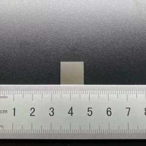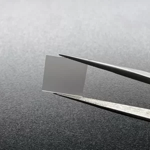
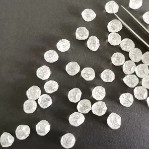
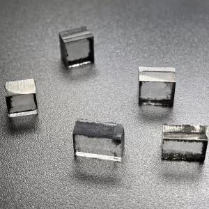
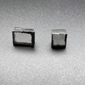
6mm*6mm CVD Lab Grown Diamond Plates 100 110 111 Crystal Orientation
6mm*6mm Square Shape Optical Grade CVD Lab Grown Diamond Plates
CVD Lab Grown Diamond Plates Description
The chemical vapor deposition (CVD) method uses the carbon gas source (generally methane + hydrogen) as the raw material, through a certain amount of energy input (microwave, hot wire, DC, etc.), produces a plasma under a certain pressure, in which the carbon gas is decomposed, the hydrocarbon bond is broken, the carbon carbon bond in the diamond structure is formed, and the carbon carbon bond is continuously combined to make it “grow up”, This method has the advantages of fast synthesis rate (higher than high temperature and high pressure method), high quality (impurities can be avoided) and easy control (different crystal planes and different kinds of diamonds can be made by adjusting the process parameters).
The methods of CVD are also divided according to the different ways of providing energy. The input energy in the form of microwave is called MPCVD; HFCVD is a method of heating the hot wire to provide energy by applying high pressure on both sides of the hot wire; Another is to apply DC voltage to the cathode and anode, and the gas will be ejected from the anode nozzle at high speed to form a plasma jet after being heated. The heating mode is dc-cvd in the form of jet. The most promising among the three is MPCVD method, which can produce diamond with high purity and good quality, and its performance is comparable to or even better than natural diamond.
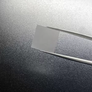
Surface: As Grown Or Laser Cut
Thickness: 0.5mm
Edge: Laser Cut or Polished
Size: 6*6mm, can customize
Application: For Making Tools
Crystal Orientation: 100 110 111
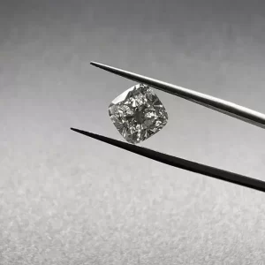
CVD Lab Grown Diamond Plates
In this article, we will discuss some of the characteristics of CVD Lab Grown Diamond Plates. These include dislocations, crystallinity, and surface roughness. We will also discuss the thermal properties and surface roughness. This article is an introduction to the world of diamond growth, and we will also discuss the advantages and disadvantages of CVD Diamond Plates. Read on for more information!
Dislocations
Achieving the desired structural properties of CVD diamond wafers has been one of the key challenges in this field. While dislocations in CVD grown active device layers do not influence electrical properties, they can have detrimental effects on the performance of these devices. To address this issue, thermal annealing has been studied for stacking faults and dislocations. Dislocations in diamonds have also been linked to the optical center “band A” that is attributed to threading mixed dislocations.
Using dislocation vector analysis, one can optimize the growth of diamond substrates. The data can be obtained by analyzing four films containing dislocations. It can also be obtained by analyzing the total X-ray extinction and absorption. Dislocations are the primary source of a wide range of variations in CVD diamonds. Further analysis of the dislocations can help to find the best growth conditions for diamond substrates.
In addition to reducing the thermal conductivity, increasing the number of dislocations on CVD diamonds also reduces optical transparency. Point defects affect photon absorption, while dislocations disrupt the cubic symmetry of the lattice. Moreover, dislocations cause local birefringence. Therefore, it is important to understand the structure of diamond plates in order to maximize the properties of these diamonds.
Thermal properties
The thermal properties of CVD Lab grown diamond plates 100, 110, and 111 are characterized by the differences in their peak X-ray diffraction (XRD) spectra. The differences in these properties are attributed to the different crystal structures present in the CVD films. Specifically, the XRD spectra of 100, 110, and 111 show an increased ratio between the G and T bands and the areas of diamond peak.
By manipulating the grain size and orientation of the diamond film, the present invention can produce a better thermal conductivity in the PVD films than in conventional methods. This is achieved by growing diamond on a nanopatterned substrate with features on the order of the initial grain size of the diamond film. Furthermore, the nanopatterned substrate can be designed to control the microstructure of the diamond film, which in turn can enhance its thermal conductivity. The degree of preferential orientation texture 110 varies with the nanoscale features.
The growth of diamond on the CVD substrates depends on a complex process of metastable competition between hydrogen etching and methyl radical deposition. In this process, the amount of methane in the gas source correlates with the growth rate and the number of holes on the diamond surface. The methane content was measured using a laser and was determined to be 0.5 mm thick.
Crystallinity
The process of creating diamonds employs several chemical processes to form polycrystalline, low-index crystals. The crystallinity of CVD Lab grown diamond plates is controlled by the growth rate of the main low-index crystalline faces of 100, 111, and 311. According to the laws of crystal growth, the area fraction of the growth-slowest face increases with increasing crystallinity.
In the first step, a patterned resist mask was used to save selected nucleation sites. During the second step, the unmasked part of the substrate was etched away. The etching process destroyed the nuclei present in this region. The pattern with integrated nuclei has four faces and a pyramid shape. As the process continues, the nuclei merge with the neighbors to form a continuous film.
In a carbon containing environment, hydrocarbon radicals attach to the lattice of the diamond. A suitable carbon content will cause the nuclei to grow in the desired crystal structure. The relative deposition rate of different planes and conditions of the plasma determines the specific growth process. As a free surface, scale enlargement is inevitable in both lateral and vertical directions.
Under low power density and high methane concentration, renucleation processes dominate. The observed film morphology can be explained by the competitive nature of CHx species with H atoms. Despite their high abundance, CH3 radicals play a crucial role in the growth of diamonds. This radical has an exceptionally large surface area and is difficult to couple to a free bond.
Surface roughness
CVD single crystal diamond materials are produced by a process in which the growth rate of the material is regulated by monitoring the processing parameters. The “a parameter” is proportional to the growth rate in direction 001 and 111. The “a” value is three times the GR in direction 001. For CVD single crystal diamond materials, the “a” value is three times the GR in direction 111.
The surfaces of single crystal diamonds are very difficult to polish. To reduce surface roughness, a Logitech Tribo Chemical Mechanical Polishing system was used. The system comprises a Logitech SF1 Syton and a polyurethane/polyester polishing pad. The polishing pad reduced the roughness of the 100 and 111 diamonds by reducing the fracturing of single crystal diamond surfaces.
Dislocations form along the edges of the growth surface of the first diamond substrate. These dislocations propagate through the diamond material in the growth direction, thereby forming the outline of the starting substrate. In some sections of the diamond plate, there are no dislocations, while other sections have many dislocations. A high degree of dislocation density indicates a rough surface. The roughness of the diamond plate depends on the surface roughness and the substrate’s shape.
The surface roughness of CVD grown diamond plates 100, 110, and 111 depends on the type of CVD growth technique used. Asymmetrical CVD growth method uses a substrate that is irregularly shaped and has a higher aspect ratio. The higher aspect ratio makes CVD growth more advantageous and provides increased lateral dimensions. During this process, the surface of the CVD grown diamond material is substantially square and has four edges.
Cost
The growing demand for CVD diamonds means that various applications are being developed. These include radiation detectors, optical components for lasers, windows for RF transmission, electrochemical sensing, ozone generation, direct oxidation of organic matter, and high power electronics. CVD diamonds are also being tested for applications in photonics and the nuclear industry. Depending on their properties, CVD diamonds can even be used for semiconductor manufacturing.
The properties of diamond make it an excellent semiconductor. The lowest losses are about 75%, which is equivalent to saving 10 MW of energy on a 300 MW HVDC converter. Despite these advantages, diamond still faces a number of challenges, including high temperature, high density, and large volume. Using diamonds in these applications allows the manufacturing industry to improve its process and make it cost competitive with other WBG materials.
The CVD process was first developed in 1952. In the 1980s, researchers reported work leading to industrial processes. Recently, however, hydrothermal synthesis was also reported. This method has been used to produce large diamond films. But this method is still not widely adopted. The latest progress in large-scale diamond film synthesis is summarized below. If you are interested in learning more about CVD and its applications, be sure to check out the resources in this article.
Availability
CVD lab grown diamond plates are a great choice for a variety of applications. They are extremely hard, possess excellent thermal conductivity, and have great chemical, pressure, and electrical resistance. They are also available in tool and thermal grades. Among the two, Tool Grade is more conductive and can be an excellent choice for certain applications. In addition, Tool Grade is available at a lower cost.
CVD diamond has a wide range of applications, including electronic doping, increasing single crystal size, and cost reduction. In the future, new users will be addressing the challenges of integration and will develop techniques to improve metallization and control strain in lasers, as well as packaging for electronics. The CVD diamond technology is bringing new solutions for many challenging applications. The following is a list of some of the applications that can benefit from CVD grown diamond.
In addition to their structural similarity, CVD scientists can control the concentration of atomic hydrogen and boron during the growth process. They can also control the charge of the defect complexes, which may result in colour changes in CVD diamond. Khan et al., a research group from the University of Washington, reported similar effects when a CVD diamond is grown with atoms of boron.
6mm*6mm CVD Lab Grown Diamond Plates 100 110 111 Crystal Orientation