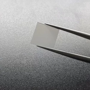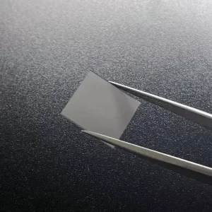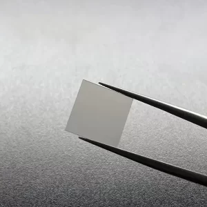
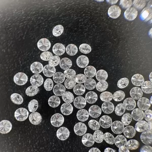
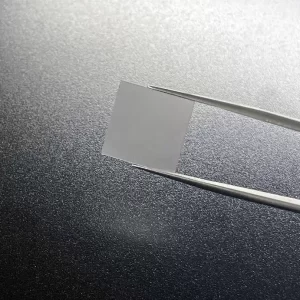
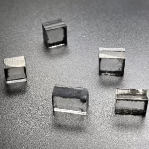
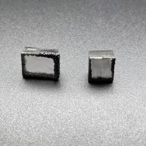
12mm*12mm CVD Single Crystal Diamonds Electronic Grade
12mm*12mm Square Shape Electronic Grade CVD Single Crystal Diamonds
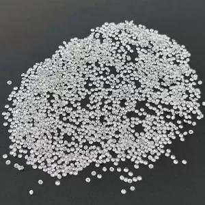
CVD Single Crystal Diamonds Description
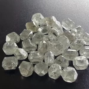
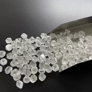
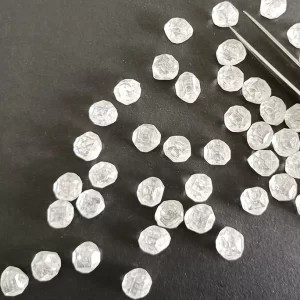
Diamond is widely used because of its excellent properties, such as the highest hardness, excellent wear resistance, low friction coefficient, high thermal conductivity, low thermal expansion coefficient and extremely stable chemical properties. CVD diamond single crystal is planar, with clear crystal edge and vertex angle.
Chemical vapor deposition (CVD) synthetic diamond products are manufactured by chemical vapor deposition (CVD) process. In the manufacturing process, the growth conditions and quality control procedures are strictly controlled.
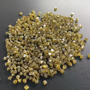
The CVD Diamond Prepared by DC arc plasma jet system is light yellow green and translucent.
It is a pure diamond with polycrystalline structure and does not contain any metallic and nonmetallic agglomerations.
It has high transmittance, high thermal conductivity, especially high wear resistance. It is the best substitute for natural diamond and synthetic diamond. It is used in processing environments requiring high wear resistance and reat dissipation.
Surface: As Grown Or Laser Cut
Thickness: 0.5mm
Edge: Laser Cut or Polished
Size: 12*12mm, can customize
Application: For Making Tools
Crystal Orientation: 100 110 111
CVD Single Crystal Diamonds Electronic Grade
What is a CVD Single Crystal Diamond? A CVD diamond may be single or multiple crystals. They may be characterized by their XRD or FE peak, Electrical conductivity, or Radiation detection. The FE peak is an electrical property that indicates a diamond’s purity. A CVD diamond may also exhibit low resistivity at low applied fields, which is a sign of crystal perfection.
XRD confirms that the CVD diamonds are single crystals
The XRD pattern reveals that CVD diamonds are single crystals, exhibiting a half-maximum width of 0.13deg. They are also highly crystalline and exhibit a sharp 111-shaped crack. CVD diamonds grow at a lower temperature than the standard processes, and they exhibit a growth rate of 10 mm/h instead of the standard process’s 0.3-mm/h growth rate.
XRD confirms that CVD single-crystal diamonds are electronic grade by confirming the crystallization of carbon atoms by chemical vapor deposition. This type of growth occurs at the interface between the film and gas phase and involves creation of dangling bonds through abstraction of hydrogen from a hydrogen stabilized surface. Hydrocarbon radicals in the gas phase are then absorbed and incorporated into the diamond crystal lattice.
XRD also shows that MPCVD produces high-growth rate, colorless single crystals. They can range from 50 to 150 mm in size, depending on the stage and the concentration of methane used. In addition to its high growth rate, MPCVD diamonds are used for the enlargement of anvils and ultrahigh-pressure compression of large samples.
In addition to the chemical analysis, the XRD results show that the x-rays reveal the nitrogen-doped CVD diamonds are electronic-grade. The nitrogen-vacancy-hydrogen defect is responsible for the colour of CVD diamond. The N-VH defect is responsible for the brown colour. Further, XRD confirms that the CVD single crystal diamonds are electronic-grade, and X-ray diffraction tests show that these diamonds are a good example of the CVD method.
The TEM image of a new sample also reveals a continuous single crystal diamond layer with a height of 1.8 nm and width of 257 nm. This layer was formed during the first five seconds after BEN termination. This short growth time rules out the coalescence of individual islands. It also suggests a crystalline connection inside the carbon layer. This is an encouraging development for CVD technology and research.
FE peak
CVD Single Crystal Diamonds exhibit a high-quality FE peak due to their uniformity and purity. In the present study, the Raman spectra of diamonds were analyzed. The diamonds were found to exhibit a broad Raman peak in a series, with a shift from 2.7 cm-1 to 4.3 cm-1. This shift can be caused by defects or nonuniform stresses. The stress may be either tensile or compressive, or both. In both cases, the peak is corresponding to a diamond on a 100-facet film.
The FE peak is characterized by broad bands of spectral intensities on different faces of the diamond. The broad bands of intensity in the Raman spectrum are due to the presence of H3 defect center in the crystal structure. These broad bands were normalized to 1332.5 cm-1 peak intensity. The peak intensity in this spectrum is higher than the FE peak of a CVD Single Crystal Diamond.
During the growth process, the impurity nitrogen plays a vital role. As the nitrogen incorporation efficiency is low, it concentrates on the growing surface. It also contaminates the growth steps and induces surface roughness. It also facilitates the incorporation of impurities. Hence, growth hillocks can lead to current leakage and a decrease in diamond electronic grade. Bilayer micro/nanocrystalline diamond coatings are free from this defect.
These findings have important implications for the design of the FE spectra of diamonds. They show the potential of CVD Single Crystal Diamonds as a wafer-size material. Moreover, CVD Single Crystal Diamonds may also serve as a platform for the fabrication of nanostructured carbon materials. However, the absence of ion bombardment complicates the process. In such a scenario, ion bombardment is a viable alternative to the current BEN synthesis.
Electrical conductivity
In this study, the electrical conductivity of CVD single crystal diamonds was studied by measuring the resistivity at different temperatures. The density of states in the Fermi level ranged from 0.22 eV/cm3 to 1.7 eV/cm3, the hopping energy W was 43.5 meV to 142.3 meV, and the average hopping distance R was between 1.49 x 10⁻⁵cm and 2.56 x 10⁻⁵cm. The hopping distance R depends strongly on the preferential orientation of the diamond film.
The thermal conductivity of CVD single crystal diamonds is comparable to that of natural diamonds. The thermal conductivity of these diamonds is similar to that of the best single-crystal diamonds. Electron mobility in CVD diamond films is approximately ten times greater than in single-crystal natural diamonds. Moreover, a single-crystal CVD diamond can be used as a platform for solid-state lasers and high-power diodes.
Electron-electron scattering and thermal conductivity have been studied by various researchers. A recent study by C. T. Walker and J. E. Graebner showed an unusually high thermal conductivity of diamond films. Another study by R. J. Jenkins investigated the thermal conductivity of amorphous solids above a plateau. Other recent studies include work by W. J. Parker, W. M. Banholzer, and Y. Aikawa.
In addition, CVD single crystal diamonds possess a high electrical conductivity due to the reduced ohmic contact resistance. This property increases the sensitivity of the sensor. A low contact resistance reduces the power loss in thermal cavitation actuators. In addition, these diamonds can serve as electrode substrates for biosensors. They can also serve as practical multilayer capacitors in wear sensors.
Radiation detection
This paper describes a new type of radiation detector that uses graphitic wire arrays fabricated at different depths within diamonds. One array of wires has a modulated bias voltage, while the other has a series of readout electrodes. Under the influence of the modulated electrical bias, X-rays passing through the detector generate charge carriers in the bulk diamond, which then travel to the nearest readout electrode. Each of the two arrays is made up of eleven electrodes spaced approximately 50 um apart.
To test the effectiveness of the radiation detector, the ionized diamond sample was irradiated using a 5 MeV proton beam. The radiation induced damage in the lattice of the diamond, and the beam penetrated the entire thickness of the diamond. In this study, the amount of radiation that the sample was exposed to was estimated at 1.85 MeV, with defects occurring throughout the sample’s depth. Gamma and neutron radiation produce point and cluster defects, respectively. However, protons produce both kinds of defects, and thus are considered to be better for testing the radiation-hardness of the detector.
The study of radiation-damaged diamonds is aimed at understanding the bulk charge transport properties of these crystals, and at understanding the thermal evolution of crystal defects. Because this technology is practical, it is now widely used in devices. But before implementing it into the real world, it is essential to test the CVD diamond’s ionization energy. This way, it can be ensured that the detector will not be tainted by light.
Another study conducted on the diamonds has shown that diamonds can be used as radiation detectors. Because of their high intrinsic purity, they can be used as a solid state ionisation chamber. They have low atomic numbers and low intrinsic carrier fraction. The diamond is an ideal choice for this type of radiation detector. It will enable the detection of various radiations in very high temperatures. The new findings are important to the advancement of the diamond technology.
Applications
One of the most promising uses of CVD Single Crystal Diamonds is in the field of optics. Single crystal CVD diamonds exhibit low birefringence due to their controlled growth and careful substrate selection. Low birefringence diamonds have the ability to improve the performance of semiconductor disk lasers and doped dielectric lasers. CVD Single Crystal Diamonds also offer excellent thermal management capabilities. Here are some of the benefits of CVD Single Crystal Diamonds in these industries.
The most important benefit of a CVD Diamond for electronic devices is its low losses. This property allows it to perform electrically in high voltage fields without affecting the performance of other materials. This is particularly advantageous in power device applications. Single Crystal Diamonds Electronic Grade applications
In addition to reducing impurity levels, CVD Single Crystal Diamonds offer a lower growth temperature than conventional processes. Oxygen also helps in removing nitrogen-related impurities. The result is a lower growth rate of 10 mm/h, which is far higher than the 0.3 mm/h of a standard process. Further, CVD Diamonds are a great option for electronic devices.
Single Crystal Diamonds are also difficult to measure. The high atomic density and rigid structure of diamond lattice leave little space for foreign atoms. Nonetheless, small substitutional defects can form in the single crystal. These defects act as electron acceptors or donors. Single Crystal Diamonds can contain Si, P, and S atoms. In addition to carbon, these non-carbon atoms also play a major role in CVD Single Crystal Diamonds.
The single crystal CVD Diamonds of the invention may have high resistivity at high applied fields. The resistivity of single crystal diamonds of this type is typically greater than 1 x 10¹² O cm. Low boron content in single crystals of diamonds allows them to be conductive. Therefore, the use of these diamonds for electronic grade applications is very promising. You may be able to find a CVD Single Crystal Diamonds Electronic Grade in a variety of shapes and sizes.
12mm*12mm CVD Single Crystal Diamonds Electronic Grade